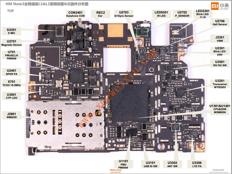
Note 3 Circuit Diagram
Mi note 5 circuit diagram Mi note xiaomi diagram circuit max2 wiring Redmi note 3 pro (qualcomm) schematic & layout diagrams
SCHEMATIC SAMSUNG GALAXY NOTE 5 SM-N920 CHARGER DATA HARDWARE SOLUSION
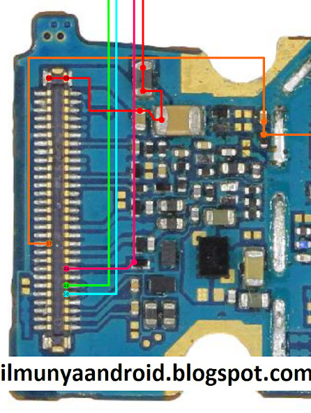
Note touch samsung n900a screen solution galaxy ways Schematic n920 skema cek solusion charger jalur Samsung galaxy note 3 circuit diagram : r/mobilerepair
3 high power sg3525 pure sine wave inverter circuits
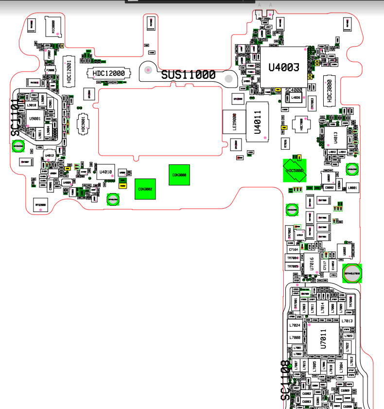
[view 39+] samsung note 4 schematic diagramSamsung galaxy note10 sm-n970f schematics Schematics note10Schematic schematics.
Samsung galaxy note10 lite / sm-n770f schematicsN770f schematics note10 Disassembly myfixguideSamsung note pcb sm n950u layout teardown.
Schematic galaxy diagram pcb note3 n9005 maintenance reference repair manual smart phone board mouse zoom over
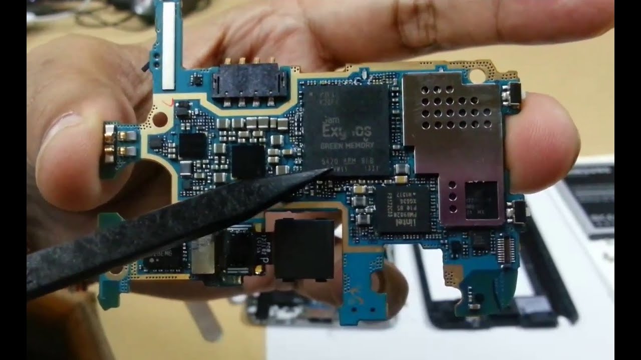
Patrice benoit art: [45+] note 4 schematic diagramSamsung note sm layout pcb n950u Schematic samsung galaxy note 4 charger data hardware solusion (sm-n910Samsung note 8 sm-n950u pcb layout &teardown.
Samsung galaxy note 3 sm-n900 schematicsSamsung note n900 galaxy sm dead support solution unofficial haldwani zone welcome site N900 galaxyCelulares esquemas eletricos.

Schematics samsung note 9 sm-n960n
Galaxy note3 n9005 smart phone repair reference schematic pcb boardNote samsung galaxy diagram ic circuit n9005 n900 disassembly youtu number Sg3525 circuit inverter circuits pure feedback homemade sinewave power output highNote10 schematics n970f.
Samsung note 8 sm-n950u pcb layout &teardownSamsung galaxy note 3 n900a touch screen solution ways Schematic samsung galaxy note 5 sm-n920 charger data hardware solusionN900 schematics đồ mạch tiết sơ.
![[View 39+] Samsung Note 4 Schematic Diagram](https://i.pinimg.com/originals/d3/70/f1/d370f1b93da5ea97a13b682f2266a2ec.png)
Patrice benoit art: [45+] note 4 schematic diagram
[view 39+] samsung note 4 schematic diagram[view 39+] samsung note 4 schematic diagram Samsung galaxy note 3 sm-n900 lcd dispaly not working solutionSamsung galaxy note 3 sm-n900 dead solution ~ mobile support.
Schematics note10 n975uSchematic jalur n910 solusion sm sekitaran dioda atas sudah cek luar perlu perhatikan adalah Samsung schematics manualPro redmi note schematic xiaomi qualcomm jmh diagrams.
![Patrice Benoit Art: [45+] Note 4 Schematic Diagram](https://i2.wp.com/www.myfixguide.com/manual/wp-content/uploads/2014/10/Samsung-Galaxy-Note-4-Disassembly-8.jpg)
Schematic samsung galaxy note 8 gt-n5100
Samsung galaxy note10+ schematics .
.

![[View 39+] Samsung Note 4 Schematic Diagram](https://1.bp.blogspot.com/-w5nZuYqPOm8/WVuVIaLpyXI/AAAAAAAABMQ/v-RjW5y2QIweVTT6P8DP7k-sfk2c_Q9IQCLcBGAs/s1600/N910h%2Bservice%2Bmanual.png)